FPGA Art Gallery
(Updated 8/19/2002)


The Gallery is a showcase of FPGA designs that Fliptronics has developed
for its clients. These pictures demonstrate examples of detailed floorplanning,
and some demonstrate very high utilization of large FPGAs (vintage 1997.
The biggest chips available now are FAR bigger). The pictures are organized
in two groups, as two different Floorplan viewers were used. The style of
each viewer is described at the top of each group. You can read more about
Floorplanning techniques in the tutorials
section.
All the Floorplan pictures can be selected to give a larger, more detailed
view.
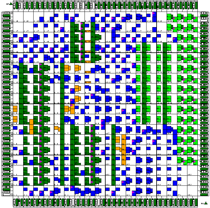
The first Gallery section is of some smaller FPGAs. In these pictures,
object that are colored light or dark green are manually Floorplanned and
placed. Objects that are colored orange are Floorplanned within themselves
(with RLOCs), but are not locked to a specific place on the chip. The final
placement for these orange structures was chosen by the FPGA placement software.
The objects that are colored blue are unstructured logic (such as state machines,
or non timing critical data path), and their placement is also unguided by
Floorplanning.
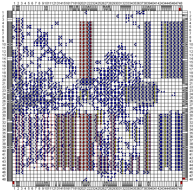
In these pictures, when viewing the full size pictures, the main black
grid is the array of CLBs (a white square). Each CLB has its usage indicated
by colored cells within the square. Colored cells on the left are the function
generators, and colored cells on the right are the flip-flops. A triangle
over a flip-flop indicates that its D input is from a function generator in
the same CLB. A thin horizontal rectangle (always green) in the bottom left
corner of a CLB square indicates that carry logic is in use.
Click for a bigger picture
|
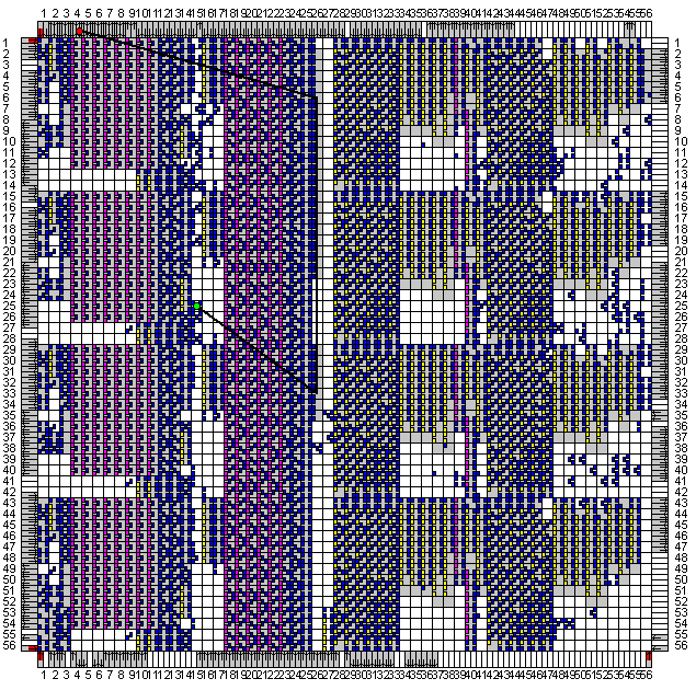
CSCANNER
The chip is an XC4008 FPGA. The blue stuff is an un-floorplanned
state machine with over 100 states. The two columns of green on the right
side are a pipelined bus interface, just to the left are 4 columns of RAM
cells (also green, 8 CLBS high). The green stuff in the top middle area are
some state counters and address registers. The lower left is a mix of 24
bit and 12 bit data path. Like most of my FPGA designs, the data path is
carefully floorplanned (the stuff in green), and the rest (state machines
and other control logic, all in blue) is left for the PPR placer to find
a suitable location for it. Detailed TimeSpecs are used to describe ALL paths
through the chip, and the design is fully synchronous. The design is in
production, and runs at speed with reasonable extra timing margins beyond
its design specification. This approach to selective floorplanning seems
to result in very short design and compile times, with quite deterministic
timing. Separate place and route runs result in almost identical timing.
|
Click for a bigger picture
|
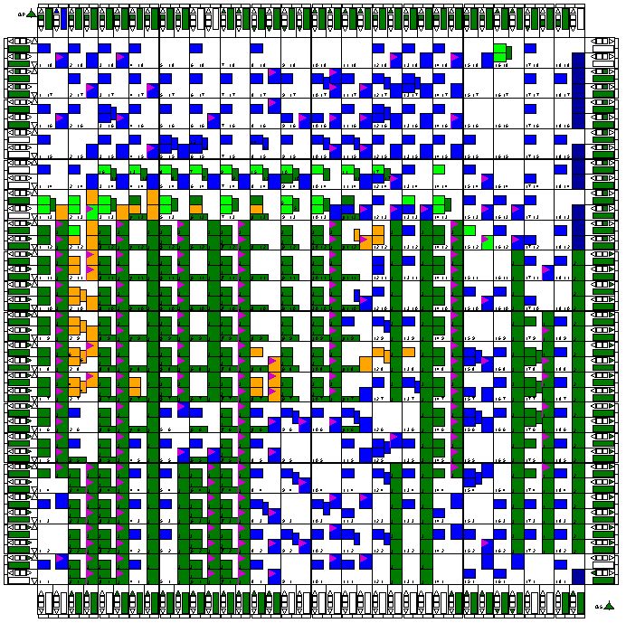
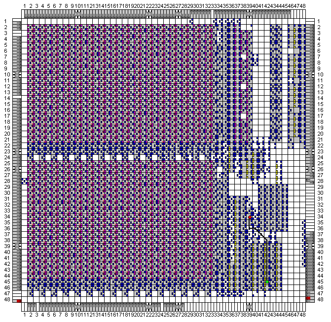
CHAINER
This chip is mostly a 24 bit data path, with some 12
bit blocks, and a very complex state machine. Green stuff is the
floor planned data path, blue stuff is the unfloorplanned statemachine.
The light green stuff is the floorplanned part of the statemachine
that directly drives control lines into the data path. For performance,
just this part of the statemachine was floorplanned (about 20%).
|
Click for a bigger picture
|
HUB_MOD
This chip implements the Interleaver and modulator
DSP for a Spread Spectrum Satellite transmitter. The I and Q portions of
the DSP are the two horizontal blocks, each 9 rows high, that are in the
top half of the chip, and span the full width. The bottom half of the chip
implements a configurable interleaver. All the light and dark green stuff
is floorplanned, the blue stuff is unfloorplanned state machine logic. |
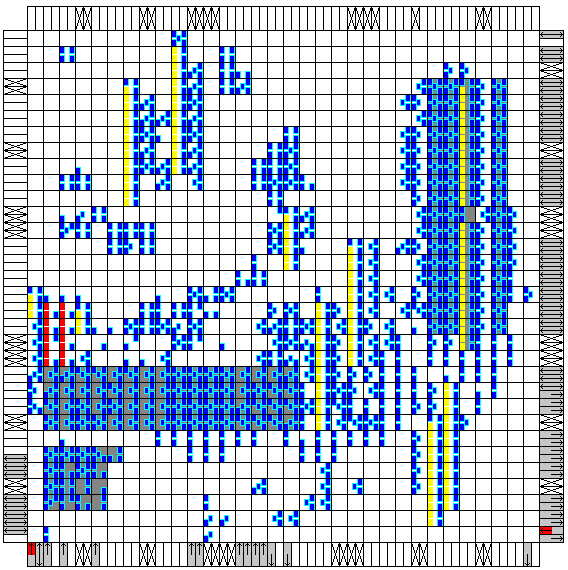
The Second Gallery section is of some more recent FPGAs.
The color coding of the following Floorplans is as follows:
If a square is empty, the CLB is not used
Within each CLB, colored squares on the left are F & G function generators,
colored squares on the right are the flip-flops, and a colored rectangle
in the middle represents the H function generator.
If a square is colored blue, then it is being used
If a square is colored yellow, then it is a function generator, and the
carry logic is active
If a square is colored magenta, then it is a function generator, and it
is being used for single ported RAM
If a square is colored red, then it is a function generator, and it is
being used for dual ported RAM
If a square is colored green, then it is a function generator, and it
is being used for ROM
If an I/O cell is colored red, then it is being used for a global clock
buffer
An "X" over an I/O cell indicates an I/O cell that is not bonded to a
package pin
An inward pointing arrow on an I/O cell indicates usage as an input
An outward pointing arrow on an I/O cell indicates usage as an output
If an I/O or CLB cell has a gray background, then it means that there
was placement control used on that location
Click for a bigger picture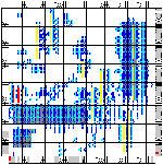
|
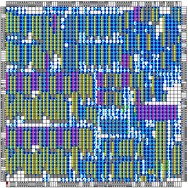
SRAMTEST
The chip is an XC4028EX and implements the
self test design that exercises the SRAM on the board. The Horizontal block
(4 rows by 16 columns) implements 16 registers that are available to the
software running on the host PC. The vertical structure on the right side
is a datapath that generates and check various test patterns while the design
is running. The blue stuff that is scattered around the chip is the state
machine that controls everything. The vertical yellow stripes are the carry
chains in various counters. The SRAM interface is on the right side, and
the CPU/ISA interface are the I/Os on the bottom and left side. |
Click for a bigger picture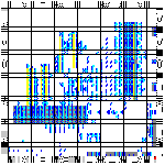
|
DRAMTEST
The chip is an XC4028EX and implements the
self test design that exercises the DRAM on the board. The Horizontal block
(4 rows by 16 columns) implements 16 registers that are available to the
software running on the host PC. The vertical structure on the right side
is a datapath that generates and check various test patterns while the design
is running. The blue stuff that is scattered around the chip is the state
machine that controls everything. The vertical yellow stripes are the carry
chains in various counters. The DRAM interface is on the right side, and
the CPU/ISA interface are the I/Os on the bottom and left side. |
Click for a bigger picture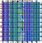
|
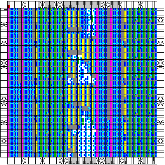
MFILT
The chip is an XC4028EX that implements two 256 stage
match filters for decoding a Spread Spectrum Satellite signal. The design
has one 256-bit by 8 equivalent shift reg with taps every other sample. It
matches against two codes being run simultaneously. This means there are
two sets of everything except the shift register. The coefficients (all
+1 or -1 ) are dynamically programmable by shifting in two new arguments
up to 128 each. The clock rate is 32MHz. The sample rate is 8MHz. The chip
rate is 4MHz. This design uses a hybrid of distributed arithmetic, serial/parallel
computation, and required very careful floorplanning. The design includes
ROMs, RAMs, carry logic, and a small amount of control logic. Operating at
32MHz, it performs 256 multiplies (8 bit) and 254 adds (9 to 15 bit) every
4 clock, delivering slightly over 4 billion operations per second. |
Click for a bigger picture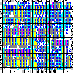
|
DVB_DEMOD
The chip is an XC4062XL that implements a DVB demodulator.
|
Click for a bigger picture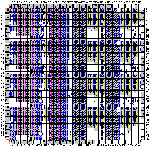
|
LINEAR
The chip is an XC4085XLA that implements a TDI Linearizer.
|
Click for a bigger picture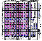
|
FORMATTER
The chip is an XC4062XLA that implements a Fibre Channel
Formatter. |
Click for a bigger picture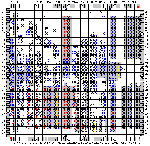
|
PCI_2_FC
The chip is an XC4062XLA that implements a full duplex
Fibre Channel to PCI-64 Interface |
Copyright © 1998, 1999, 2000, 2001, 2002 by Fliptronics.
All rights reserved.